Products+
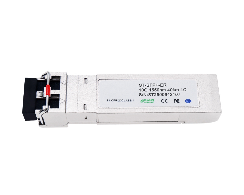
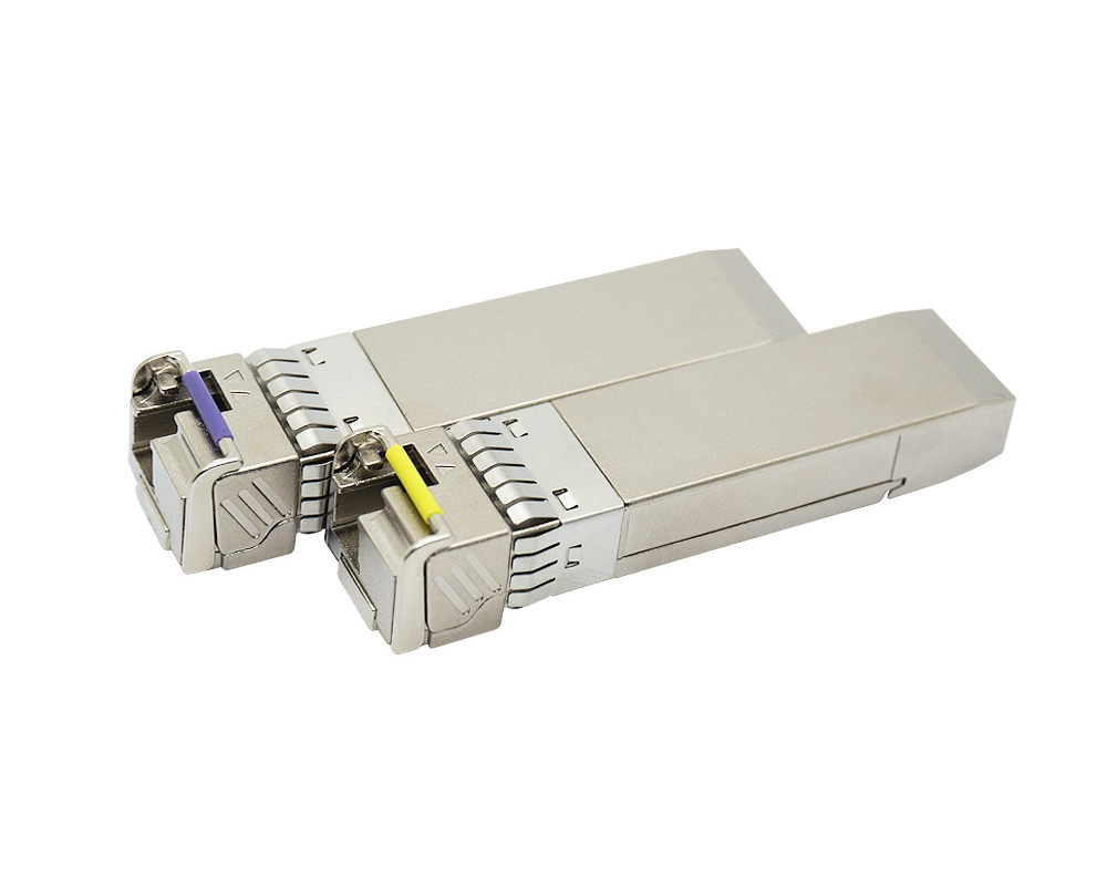
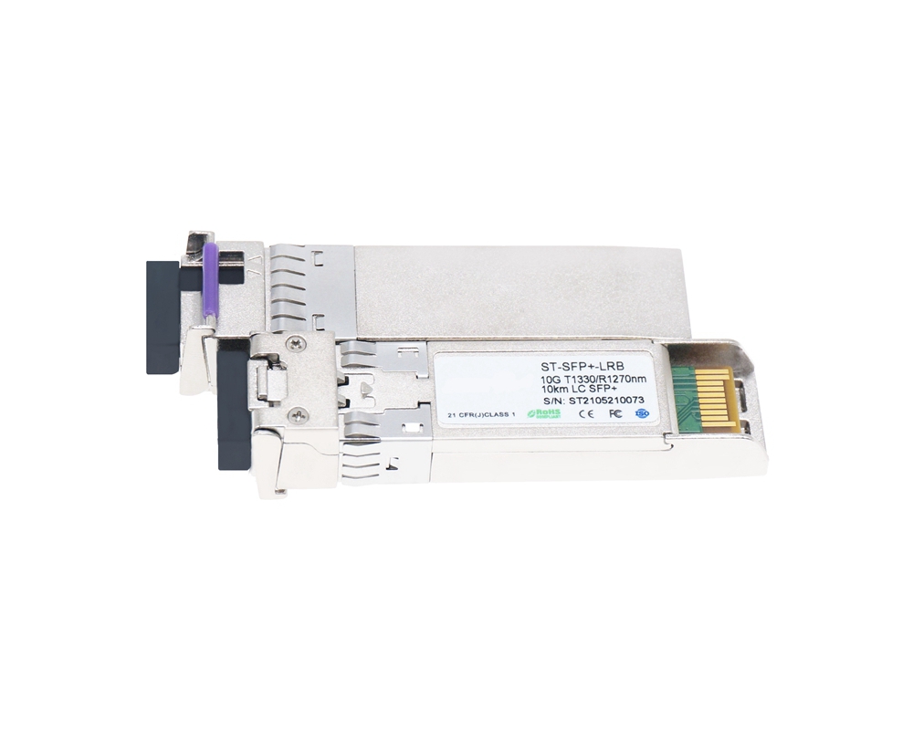
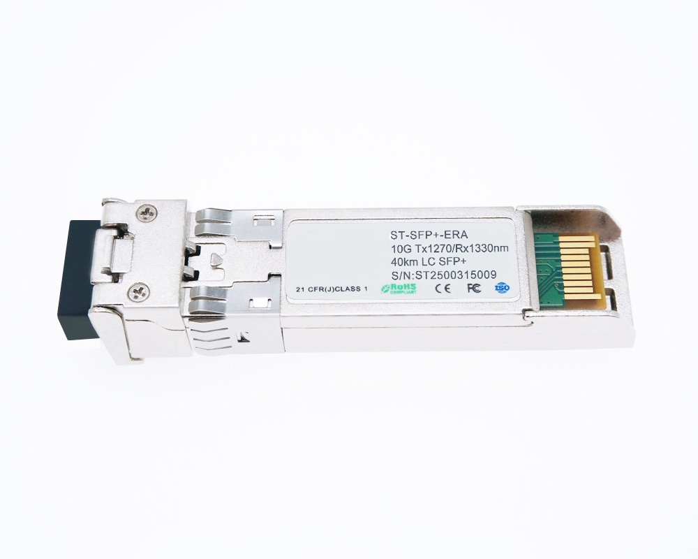
10G SFP+ ER 1550mm 40km Compatible LC Transceiver
SFP+ER Transceiver is designed for 10GBASE-ER/EW, and 8.5G/10G Fiber- Channel applications, fully tested compatible for over 100 vendors.
Features
* Compliant with SFF-8413 and IEE802.3ae
* Data rate selectable ≤4.25Gbps or 9.95Gbps to 10.3Gbps bit rates
* Cooled EML transmitter and PIN receiver
* link length up to 40km
* Low Power Dissipation 1.5W Maximum
* -5ºC to 70ºC Operating Case Temperature
* Single 3.3V power supply
* Diagnostic Performance Monitoring of module temperature, supply Voltages, laser bias current, transmit optical power, receive optical power
* RoHS compliant and lead free
Applications
* 10GBASE-ER/EW (with/without FEC)
* 10G Fiber Channel (with/without FEC)
Description
SFP+ER Transceiver is designed for 10GBASE-ER/EW, and 8.5G/10G Fiber- Channel applications.
The transceiver consists of two sections: The transmitter section incorporates a colded EML laser. And the receiver section consists of a PIN photodiode integrated with a TIA. All modules satisfy class I laser safety requirements. 6COM SFP+ER Digital diagnostics functions are available via a 2-wire serial interface, as specified in SFF-8472, which allows real-time access to device operating parameters such as transceiver temperature, laser bias current, transmitted optical power, received optical power and transceiver supply voltage.
Absolute Maximum Ratings
|
Parameter |
Symbol |
Min |
Max |
Unit |
|
Supply Voltage |
Vcc |
-0.5 |
3.8 |
V |
|
Storage Temperature |
Tst |
-40 |
85 |
ºC |
|
Relative Humidity |
Rh |
0 |
85 |
% |
Operating Conditions
|
Parameter |
Symbol |
Min |
Typical |
Max |
Unit |
|
Supply Voltage |
Vcc |
3.13 |
3.3 |
3.47 |
V |
|
Supply current |
Icc |
|
360 |
450 |
mA |
|
Operating Case temperature |
Tca |
-5 |
- |
70 |
ºC |
|
Module Power Dissipation |
Pm |
- |
1.2 |
1.5 |
W |
Notes:
[1] Supply current is shared between VCCTX and VCCRX.
[2] In-rush is defined as current level above steady state current requirements.
Transmitter Specifications – Optical
|
Parameter |
Symbol |
Min |
Typical |
Max |
Unit |
|
Center Wavelength |
lc |
1530 |
|
1565 |
pm |
|
Optical Average Power |
Po |
-3 |
- |
+3 |
dBm |
|
Optical OMA Power |
Pom |
-2.1 |
|
|
dBm |
|
Side Mode Suppression Ratio |
SMSR |
30 |
- |
- |
dB |
|
Optical Transmit Power (disabled) |
PTX_DISABLE |
- |
- |
-30 |
dBm |
|
Extinction Ratio |
ER |
6 |
|
- |
dB |
|
RIN21OMA [1] |
|
|
|
-128 |
dB/Hz |
|
Optical Return Loss Tolerance |
|
|
|
21 |
dB |
Notes:
[1] RIN measurement is made with a return loss at 21 dB.
Transmitter Specifications – Electrical
|
Parameter |
Symbol |
Min |
Typical |
Max |
Unit |
|
Data Rate |
Mra |
- |
10.3 |
11.3 |
Gbps |
|
Input differential impedance |
Rim |
- |
100 |
- |
Ω |
|
Differential data Input |
VtxDIFF |
120 |
- |
850 |
mV |
|
Transmit Disable Voltage |
VD |
2.0 |
- |
Vcc3+0.3 |
V |
|
Transmit Enable Voltage |
Ven |
0 |
- |
+0.8 |
V |
|
Transmit Disable Assert Time |
Vn |
- |
- |
100 |
us |
Receiver Specifications – Optical
|
Parameter |
Symbol |
Min |
Typical |
Max |
Unit |
|
Input Operating Wavelength |
λ |
1530 |
- |
1565 |
nm |
|
Average receive power |
|
- |
- |
-1.0 |
dBm |
|
Receiver sensitivity in OMA |
|
- |
- |
-14.1 |
dBm |
|
Stressed receiver sensitivity in OMA[1]
|
|
|
|
-11.3 |
dBm |
|
Maximum Input Power |
RX-overload |
- |
- |
-1 |
dBm |
|
Reflectance |
Rrx |
- |
- |
-27 |
dB |
|
Loss of Signal Asserted |
|
-25 |
- |
- |
dBm |
|
LOS De-Asserted |
|
- |
- |
-16 |
dBm |
|
LOS Hysteresis |
|
0.5 |
- |
- |
dB |
Notes:
[1] Measured with conformance test signal for BER = 10–12. The stressed sensitivity values in the table are for system level BER measurements which include the effects of CDR circuits. It is recommended that at least 0.4 dB additional margin be allocated if component level measurements are made
without the effects of CDR circuits.
Receiver Specifications – Electrical
|
Parameter |
Symbol |
Min |
Typical |
Max |
Unit |
|
Data Rate |
Mra |
- |
10.3 |
11.3 |
Gbps |
|
Differential Output Swing |
Vout P-P |
350 |
- |
850 |
mV |
|
Rise/Fall Time |
Tr / Tf |
24 |
- |
- |
ps |
|
Loss of Signal –Asserted |
VOH |
2 |
- |
Vcc3+0.3- |
V |
|
Loss of Signal –Negated |
VOL |
0 |
- |
+0.4 |
V |
Figure1.Electrical Pin-out Details
Pin Descriptions
|
Pin |
Symbol |
Name/Description |
|
1 |
VEET [1] |
Transmitter Ground |
|
2 |
Tx_FAULT [2] |
Transmitter Fault |
|
3 |
Tx_DIS [3] |
Transmitter Disable. Laser output disabled on high or open |
|
4 |
SDA [2] |
2-wire Serial Interface Data Line |
|
5 |
SCL [2] |
2-wire Serial Interface Clock Line |
|
6 |
MOD_ABS [4] |
Module Absent. Grounded within the module |
|
7 |
RS0 [5] |
RS0 for Rate Select: Open or Low = Module supports ≤4.25Gbps High = Module supports 9.95 Gb/s to 10.3125 Gb/s |
|
8 |
RX_LOS [2] |
Loss of Signal indication. Logic 0 indicates normal operation |
|
9 |
RS1 [5] |
No connection required |
|
10 |
VEER [1] |
Receiver Ground |
|
11 |
VEER [1] |
Receiver Ground |
|
12 |
RD- |
Receiver Inverted DATA out. AC Coupled |
|
13 |
RD+ |
Receiver DATA out. AC Coupled |
|
14 |
VEER [1] |
Receiver Ground |
|
15 |
VCCR |
Receiver Power Supply |
|
16 |
VCCT |
Transmitter Power Supply |
|
17 |
VEET [1] |
Transmitter Ground |
|
18 |
TD+ |
Transmitter DATA in. AC Coupled |
|
19 |
TD- |
Transmitter Inverted DATA in. AC Coupled |
|
20 |
VEET [1] |
Transmitter Ground |
Notes:
[1] Module circuit ground is isolated from module chassis ground within the module.
[2].should be pulled up with 4.7k – 10k ohms on host board to a voltage between 3.15Vand 3.6V.
[3]Tx_Disable is an input contact with a 4.7 kΩ to 10 kΩ pullup to VccT inside the module.
[4]Mod_ABS is connected to VeeT or VeeR in the SFP+ module. The host may pull this contact up to Vcc_Host with a resistor in the range 4.7 kΩ to10 kΩ.Mod_ABS is asserted “High” when the SFP+ module is physically absent from a host slot.
[5] RS0 and RS1 are module inputs and are pulled low to VeeT with > 30 kΩ resistors in the module.
Figure2. Host Board Power Supply Filters Circuit
Figure3. Host-Module Interface
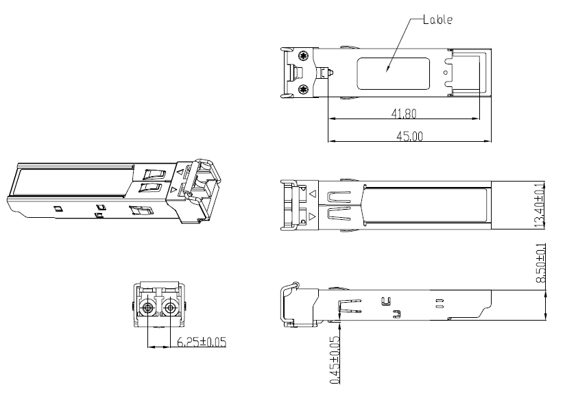
Figure6. Mechanical Specifications
Ordering information
|
Part Number |
Product Description |
|
ST-SFP+-ER |
10Gbps 1550nm SFP+ ER 40km LC, -5ºC ~ +70ºC |