Products+
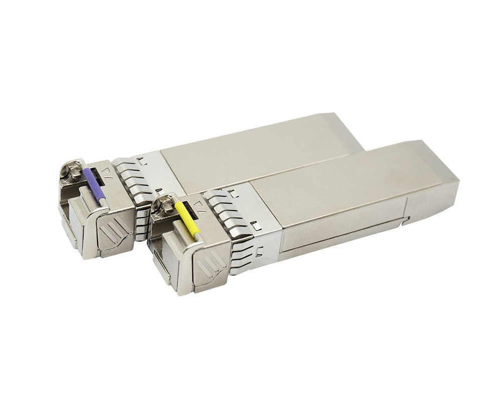
10G SFP+ LRM 1310nm 220m compatible SFP Transceiver
10G SFP+ LRM 1310nm 220m SFP Transceiver,SFP+ LRM is an optical transceiver module for transmission at 1310nm over legacy multimode fiber, fully tested compatible for over 100 vendors.
Features
* Supports 9.95 to 10.3Gbps bit rates
* Transmission distance up to 220m (OM1 fiber)
* Hot Pluggable SFP+ footprint
* 1310nm FP transmitter, PIN photo-detector
* Digital Status monitoring Interface
* Duplex LC connector
* RoHS compliant and Lead Free
* Metal enclosure for lower EMI
* Single 3.3V power supply
* Power dissipation < 1W
* Operating case temperature: 0 to 70℃
* Compliant with FC-PI-4 800-Mx-SN-I, SFF-8431 , SFF-8432 and SFF-8472
Applications
* 10GBASE-LRM 10G Ethernet
* Legacy FDDI multimode links
Product description
SFP+ LRM is an optical transceiver module for transmission at 1310nm over legacy multimode fiber. Supporting 10GBASE-LRM Ethernet standard make it ideally suited for 10G datacom. Its very low power consumption and its excellent EMI performance allow system design with high port density. The small form factor integrates a 1310nm Fabry-Perot (FP) laser in an LC package and a linear multimode PIN receiver.
This module is lead free, RoHS compliant and is designed and tested in accordance with industry safety standards.This SFP+ transceiver is a linear-interface transceiver that enables, in conjunction with an Electronic Dispersion Compensation (EDC) on the host board, an IEEE802.3aq 10GBASE-LRM compliant link. The host board EDC provides correction for the severe modal dispersion that may occur during propagation through multimode fiber links, including legacy installed FDDI multimode fiber (see IEEE802.3aq for detailed information regarding fiber coverage).
Unlike the XFP MSA transceiver requirements, the SFP+ transceiver does not contain internal retiming circuitry, and thus some of the Transmitter Optical Characteristics stated in this data sheet require that the Host Board is compliant to the SFP+ MSA specifications. See Chapter 3 in Reference [1] for further details.
Pin definition
The SFP+ modules are hot-pluggable. Hot pluggable refers to plugging in or unplugging a module while the host board is powered. The SFP+ host connector is a 0.8 mm pitch 20 position right angle improved connector specified by SFF-8083, or stacked connector with equivalent with equivalent electrical performance.
Host PCB contact assignment is shown in Figure 2 and contact definitions are given in Table 2.
SFP+ module contacts mates with the host in the order of ground, power, followed by signal as illustrated by Figure 3 and the contact sequence order listed in Table 2.
Figure 3: Module Contact Assignment
Table 2: SFP+ Module PIN Definition
Absolute maximum rating
These values represent the damage threshold of the module. Stress in excess of any of the individual Absolute Maximum Ratings can cause immediate catastrophic damage to the module even if all other parameters are within Recommended Operating Conditions.
|
Parameters |
Symbol |
Min. |
Max. |
Unit |
|
Power Supply Voltage |
VCC |
0 |
+3.6 |
V |
|
Storage Temperature |
Tc |
-40 |
+85 |
°C |
|
Operating Case Temperature |
Tc |
0 |
+70 |
°C |
|
Relative Humidity |
RH |
5 |
95 |
% |
Table 3: Absolute Maximum Rating
Recommended operating environment
Recommended Operating Environment specifies parameters for which the electrical and optical characteristics hold unless otherwise noted.
|
Parameter |
Symbol |
Min. |
Typical |
Max |
Unit |
|
Power Supply Voltage |
VCC |
3.135 |
3.300 |
3.465 |
V |
|
Operating Case Temperature |
TC |
0 |
25 |
70 |
°C |
Table 4: Recommended Operating Environment
LOW Speed Characteristics
|
Parameter |
Symbol |
Min. |
Typical |
Max |
Unit |
|
Power Consumption |
|
|
1.2 |
1.2 |
W |
|
TX_Fault,RX_LOS |
VOL |
0 |
|
0.4 |
V |
|
VOH |
Host_Vcc-0.5 |
|
Host_Vcc+0.3 |
V |
|
|
TX_DIS |
VIL |
-0.3 |
|
0.8 |
V |
|
VIH |
2.0 |
|
VCCT+0.3 |
V |
|
|
RS0,RS1 |
VIL |
-0.3 |
|
0.8 |
V |
|
VIH |
2.0 |
|
VCCT+0.3 |
V |
Electrical characteristics
|
Parameter |
Conditions |
Symbol |
Min. |
Typical |
Max |
Unit |
|
|
Nominal Data Rate |
|
VID |
|
10.3125 |
|
Gbps |
|
|
Supply Voltage |
|
Vcc |
3.14 |
|
3.46 |
V |
|
|
Supply Current |
|
Icc |
|
200 |
300 |
mA |
|
|
Power Dissipation |
|
P |
|
|
1 |
W |
|
|
Transmitter
|
|||||||
|
Input differential impedance |
2 |
Rin |
|
100 |
|
Ω |
|
|
Single ended data input swing |
3 |
Vin,pp |
90 |
|
350 |
mV |
|
|
Transmit Disable Voltage |
4 |
VD |
2 |
|
Vcc |
V |
|
|
Transmit Enable Voltage |
|
VEN |
Vee |
|
Vee+ 0.8 |
V |
|
|
Receiver |
|||||||
|
Termination Mismatch at 1 MHz |
|
ΔZM |
|
|
5 |
% |
|
|
Single Ended Output Voltage Tolerance |
|
|
-0.3 |
|
4.0 |
V |
|
|
Output AC Common Mode Voltage |
|
|
|
|
7.5 |
mV RMS |
|
|
Output Rise and Fall time (20% to 80%) |
5 |
Tr, Tf |
30 |
|
|
Ps |
|
|
Relative Noise LRM Links with crosstalk |
6 |
dRNx |
|
|
TBD equation |
dB/Hz |
|
|
Difference Waveform Distortion Penalty |
7 |
dWDP |
per SFF-8431 |
dB |
|||
|
Differential Voltage Modulation Amplitude |
|
VMA |
180 |
|
600 |
mV |
|
|
LOS Fault |
8 |
VLOS fault |
2 |
|
VccHOST |
V |
|
|
LOS Normal |
8 |
VLOS norm |
Vee |
|
Vee+ 0.8 |
V |
|
|
Power Supply Noise Tolerance |
9 |
VccT/VccR |
per SFF-8431 |
mVpp |
|||
Notes:
- Non-condensing.
- Connected directly to TX data input pins. AC coupling from pins into laser driver IC.
- Per SFF-8431 Rev 3.0
- Into 100 ohms differential termination.
- Measured with Module Compliance Test Board and OMA test pattern.
- Crosstalk source rise/fall time (20%-80%) is 35 ps.
- Defined with reference receiver with 14 T/2 spaced FFE taps and 5 T spaced DFE taps.
- LOS is an open collector output. Should be pulled up with 4.7k – 10kΩ on the host board. Normal operation is logic 0; loss of signal is logic 1. Maximum pull-up voltage is 5.5V.
- As described in Section 2.8.1, SFF-8431 Rev 3.0.
General Specifications
|
Parameter |
Symbol |
Min. |
Typical |
Max |
Unit |
Notes |
|
|
Bit Rate |
BR |
|
10.3125 |
|
Gb/sec |
1 |
|
|
Bit Error Ratio |
BER |
|
|
10-12 |
|
2 |
|
|
Maximum Supported Distances |
|||||||
|
Fiber Type |
1310nm OFL Bandwidth |
|
|
|
|
|
|
|
62.5μm |
“FDDI” 160MHz/km |
Lmax |
|
|
220 |
m |
3 |
|
OM1 200MHz/km |
|
|
220 |
||||
|
50μm |
400MHz/km |
Lmax |
|
|
100 |
m |
3 |
|
OM2 500MHz/km |
|
|
220 |
||||
|
OM3 2000MHz/km |
|
|
220 |
||||
Notes:
- 10GBASE-LRM
- Tested with a 231 – 1 PRBS
- Operating range as defined by IEEE standards. Longer reach possible depending upon link implementation.
Optical characteristics
|
Parameter |
Symbol |
Min. |
Typical |
Max |
Unit |
Notes |
|
Transmitter |
||||||
|
Center Wavelength |
λt |
1260 |
|
1355 |
nm |
|
|
RMS spectral width |
λrms @1260nm |
- |
- |
2.4 |
nm |
2 |
|
λrms @ 1260nm-1300 |
2.4 |
|||||
|
λrms @ 1300nm-1355 |
4 |
|||||
|
Average Optical Power |
Pavg |
-6.5 |
- |
0.5 |
dBm |
1 |
|
Extinction Ratio |
ER |
3.5 |
- |
- |
dB |
|
|
Optical Modulation Amplitude (OMA) |
POMA |
-4.5 |
|
+1.5 |
dBm |
|
|
Peak Launch Power |
PMAX |
|
|
3 |
dBm |
|
|
Transmitter Waveform Dispersion Penalty |
TWDP |
|
|
4.7 |
dB |
3 |
|
Average Launch power of OFF transmitter |
POFF |
|
|
-30 |
dBm |
|
|
Uncorrelated Jitter [rms] |
Txj |
|
|
0.033 |
UI |
|
|
Encircled Flux |
<5μm |
30 |
|
|
% |
|
|
<11μm |
81 |
|
|
|
||
|
Transmitter Reflectance |
|
|
|
-12 |
dB |
|
|
Optical Return Loss Tolerance |
|
20 |
|
|
dB |
|
|
Relative Intensity Noise
|
Rin |
|
|
-128 |
dB/Hz |
|
|
Receiver |
||||||
|
Comprehensive Stressed Receiver Sensitivity (OMA) @ 10.3125Gb/s |
Precursor |
- |
- |
-6.5 |
dBm |
5 |
|
Symmetrical |
|
|
-6 |
dBm |
||
|
Postcursor |
|
|
-6.5 |
dBm |
||
|
LOS Assert |
LosA |
-30 |
- |
|
dBm |
|
|
LOS De-assert |
LosD |
|
|
-11 |
dBm |
|
|
Overload |
PMAX |
-+1.5 |
- |
|
dBm |
4 |
|
Receiver Reflectance |
|
- |
- |
-12 |
dB |
|
|
LOS Hysteresis |
|
0.5 |
|
|
dB |
|
Notes:
- Average power figures are informative only, per IEEE802.3aq
- Maximum RMS spectral width as specified by Figure 3
- Optical Eye Mask requires the host board to be SFF-8431 compliant. Optical eye mask per IEEE802.3aq.
- TWDP figure requires the host board to be SFF-8431compliant. TWDP is calculated using the Matlab code provided in clause 68.6.6.2 of IEEE802.3aq
- Receiver overload specified in OMA and under the worst comprehensive stressed condition.
- Conditions of stressed receiver tests per IEEE802.3aq. CSRS testing requires the host board to be SFF-8431 compliant.
Digital Diagnostic Functions
The following digital diagnostic characteristics are defined over the Recommended Operating Environment unless otherwise specified. It is compliant to SFF8472 Rev9.2 with internal calibration mode. For external calibration mode please contact our sales stuff.a
|
Parameter |
Symbol |
Min. |
Max |
Unit |
Notes |
|
Accuracy |
|||||
|
Transceiver Temperature |
DMI_Temp |
-3 |
+3 |
degC |
Over operating temp |
|
TX Output optical power |
DMI_TX |
-3 |
+3 |
dB |
|
|
RX Input optical power |
DMI_RX |
-3 |
+3 |
dB |
-3dBm to -12dBm range |
|
Transceiver Supply voltage |
DMI_VCC |
-0.08 |
+0.08 |
V |
Full operating range |
|
Bias current monitor |
DMI_Ibias |
-10% |
10% |
mA |
|
|
Dynamic Range Accuracy |
|||||
|
Transceiver Temperature |
DMI_Temp |
-5 |
70 |
degC |
|
|
TX Output optical power |
DMI_TX |
-9 |
-1 |
dBm |
|
|
RX Input optical power |
DMI_RX |
-18 |
0 |
dBm |
|
|
Transceiver Supply voltage |
DMI_VCC |
3.0 |
3.6 |
V |
|
|
Bias current monitor |
DMI_Ibias |
0 |
16 |
mA |
|
Control and status I/O timing characteristics
Timing characteristics of control and status I/O are included in Table 8, which is also defined in SFF-8431.
Table 8: Timing Characteristics
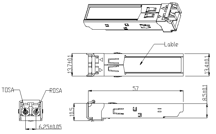
Mechanical
Table 9: Key Mechanical Dimensions
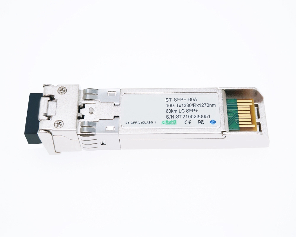
Ordering information
|
Part Number |
Description |
|
ST-SFP+-LRM |
10G 1310nm 220m LC SFP+ Transceiver 0ºC ~ +70ºC |