Products+
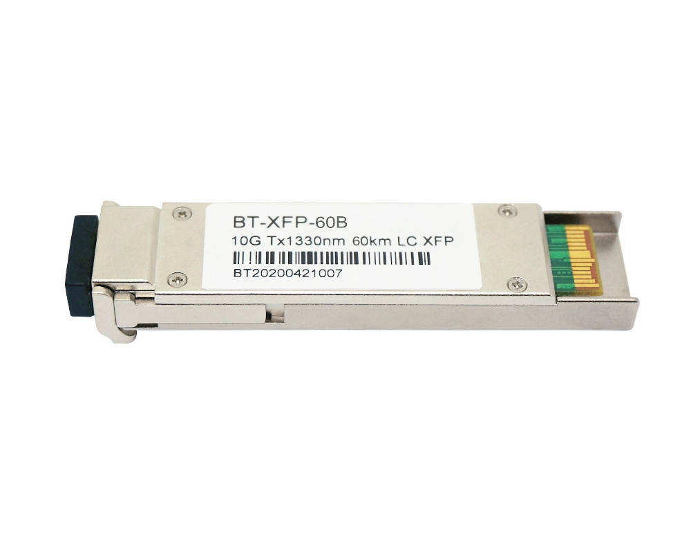
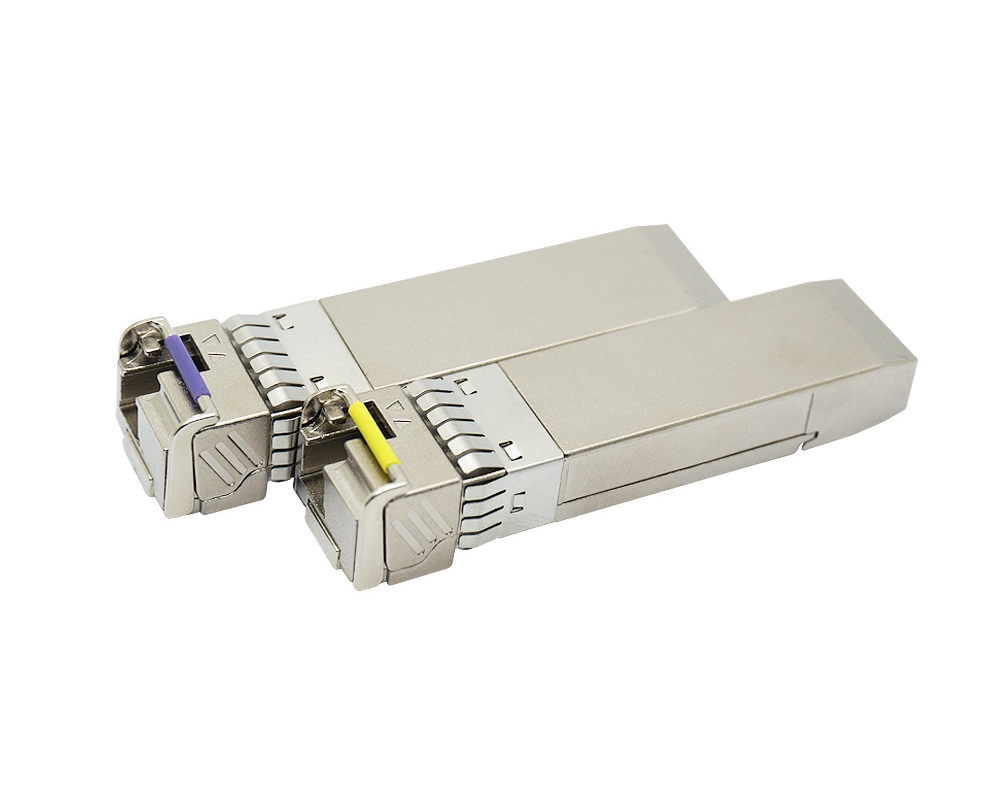
10G 1270/1330nm 60km Compatible XFP Bi-Directional Transceiver
10Gbps 1270/1330nm 60km XFP Bi-Directional Transceiver,fully tested compatible for over 100 vendors.
PRODUCT FEATURES
- Up to 10.7Gbps Data Links
- Single Mode LC Receptacle Bi-directional Transceiver
- Up to 60km transmission on SMF
- Power dissipation<1.5W
- 1270nm DFB laser and 1330nm PIN receiver
- 2-wire interface with integrated Digital Diagnostic monitoring
- EEPROM with Serial ID Functionality
- Compliant with FC_PI_4 REV 7.0
- Compliant with XFP MSA with duplex LC connector
- Single + 3.3V Power Supply and LVTTL Logic
Operating case temperature:0~+70ºC
APPLICATIONS
- 10GBASE-BX 10.3125Gb/s Ethernet
- 10GBASE-BX 9.953Gb/s Ethernet
- SONET OC-192 SR-1 SDH STM I-64.1
PRODUCT DESCRIPTION
The transceiver is hot pluggable 3.3V Small-Form-Factor transceiver module. It designed expressly for high-speed communication applications that require rates up to 10.7Gb/s, it designed to be compliant with XFP MSA. The module data link up to 60km in 9/125um single mode fiber.
The optical output can be disabled by a LVTTL logic high-level input of Tx Disable. Tx Fault is provided to indicate that degradation of the laser. Loss of signal (LOS) output is provided to indicate the loss of an input optical signal of receiver or the link status with partner.
Absolute Maximum Ratings
|
Parameter |
Symbol |
Min. |
Typ. |
Max. |
Unit |
Note |
|
Storage Temperature |
Ts |
-40 |
- |
85 |
ºC |
|
|
Storage Ambient Humidity |
HA |
5 |
- |
95 |
% |
|
|
Operating Relative Humidity |
RH |
- |
- |
85 |
% |
|
|
Power Supply Voltage |
VCC |
-0.3 |
- |
4 |
V |
|
|
Signal Input Voltage |
VCC |
Vcc-0.3 |
- |
Vcc+0.3 |
V |
|
Recommended Operating Conditions
|
Parameter |
Symbol |
Min. |
Typ. |
Max. |
Unit |
Note |
|
Ambient Operating Temperature |
TA |
0 |
- |
70 |
ºC |
Without air flow |
|
Power Supply Voltage |
VCC |
3.14 |
3.3 |
3.47 |
V |
|
|
Power Supply Current |
ICC |
- |
- |
450 |
mA |
|
|
Data Rate |
BR |
|
10.3125 |
|
Gbps |
|
|
Transmission Distance |
TD |
2 |
- |
60 |
km |
Note (1) |
|
Coupled fiber |
Single mode fiber |
ITU-T G.652 |
||||
Note (1). Measured with SMF
Specification of Transmitter
|
Parameter |
Symbol |
Min. |
Typ. |
Max. |
Unit |
Note |
|
Average Launched Power |
PO |
-2 |
- |
2 |
dBm |
|
|
Average Launched Power(Laser Off) |
POUT-OFF |
- |
- |
-30 |
dBm |
Note (1) |
|
Optical Modulation Amplitude |
OMA |
-3 |
- |
- |
dBm |
Note (1) |
|
Center Wavelength Range |
λC |
1260 |
1270 |
1280 |
nm |
|
|
Side mode suppression ratio |
SMSR |
30 |
- |
- |
dB |
|
|
Spectrum Bandwidth(-20dB) |
σ |
- |
- |
1 |
nm |
|
|
Extinction Ratio |
ER |
3.5 |
6 |
- |
dB |
Note (2) |
|
Output Eye Mask |
Compliant with FC_PI_4 REV 7.0 |
|
Note (2) |
|||
Note (1).The optical power is launched into SMF
Note (2). Measured with RPBS 2^31-1 test pattern @10.3125Gbs
Specification of Receiver
|
Parameter |
Symbol |
Min. |
Typ. |
Max. |
Unit |
Note |
|
Input Optical Wavelength |
λIN |
1320 |
1330 |
1340 |
nm |
|
|
Receiver Sensitivity in average |
PIN |
- |
- |
-15 |
dBm |
Note (1) |
|
Input Saturation Power (Overload) |
PSAT |
0.5 |
- |
- |
dBm |
Note (1) |
|
LOS -Assert Power |
PA |
-30 |
- |
- |
dBm |
|
|
LOS -Deassert Power |
PD |
- |
- |
-18 |
dBm |
|
|
LOS -Hysteresis |
PHys |
0.5 |
- |
4 |
dB |
|
Note (1). Measured with RPBS 2^31-1 test pattern @10.3125Gbs BER=<10^-12 ER=6DB
Electrical Interface Characteristics
|
Parameter |
Symbol |
Min. |
Typ. |
Max. |
Unit |
Note |
|
Total power supply current |
Icc |
- |
- |
350 |
mA |
|
|
Transmitter |
||||||
|
Differential Data Input Voltage |
VDT |
120 |
- |
820 |
mVp-p |
|
|
Differential line input Impedance |
RIN |
85 |
100 |
115 |
Ohm |
|
|
Transmitter Fault Output-High |
VFaultH |
2.4 |
- |
Vcc |
V |
|
|
Transmitter Fault Output-Low |
VFaultL |
-0.3 |
- |
0.8 |
V |
|
|
Transmitter Disable Voltage- High |
VDisH |
2 |
- |
Vcc+0.3 |
V |
|
|
Transmitter Disable Voltage- low |
VDisL |
-0.3 |
- |
0.8 |
V |
|
|
Receiver |
||||||
|
Differential Data Output Voltage |
VDR |
300 |
- |
850 |
mVp-p |
|
|
Differential line Output Impedance |
ROUT |
80 |
100 |
120 |
Ohm |
|
|
Receiver LOS Pull up Resistor |
RLOS |
4.7 |
- |
10 |
KOhm |
|
|
Data Output Rise/Fall time |
tr/tf |
20 |
- |
- |
ps |
|
|
LOS Output Voltage-High |
VLOSH |
2 |
- |
Vcc |
V |
|
|
LOS Output Voltage-Low |
VLOSL |
-0.3 |
- |
0.4 |
V |
|
Pin Description
|
Pin |
Logic |
Symbol |
Name/Description |
Note |
|
1 |
|
GND |
Module Ground |
1 |
|
2 |
|
VEE5 |
Optional –5.2 Power Supply – Not required |
|
|
3 |
LVTTL-I |
Mod-Desel |
Module De-select; When held low allows the module to respond to 2-wire serial interface commands |
|
|
4 |
LVTTL-O |
Interrupt |
Interrupt (bar); Indicates presence of an important condition which can be read over the serial 2-wire interface |
2 |
|
5 |
LVTTL-I |
TX_DIS |
Transmitter Disable; Transmitter laser source turned off |
|
|
6 |
|
VCC5 |
+5 Power Supply |
|
|
7 |
|
GND |
Module Ground |
1 |
|
8 |
|
VCC3 |
+3.3V Power Supply |
|
|
9 |
|
VCC3 |
+3.3V Power Supply |
|
|
10 |
LVTTL-I |
SCL |
Serial 2-wire interface clock |
2 |
|
11 |
LVTTLI/O |
SDA |
Serial 2-wire interface data line |
2 |
|
12 |
LVTTL-O |
Mod_Abs |
Module Absent; Indicates module is not present. Grounded in the module. |
2 |
|
13 |
LVTTL-O |
Mod_NR |
Module Not Ready; BTON defines it as a logical OR between RX_LOS and Loss of Lock in TX/RX. |
2 |
|
14 |
LVTTL-O |
RX_LOS |
Receiver Loss of Signal indicator |
2 |
|
15 |
|
GND |
Module Ground |
1 |
|
16 |
|
GND |
Module Ground |
1 |
|
17 |
CML-O |
RD- |
Receiver inverted data output |
|
|
18 |
CML-O |
RD+ |
Receiver non-inverted data output |
|
|
19 |
|
GND |
Module Ground |
1 |
|
20 |
|
VCC2 |
+1.8V Power Supply – Not required |
|
|
21 |
LVTTL-I |
P_Down/RST |
Power Down; When high, places the module in the low power stand-by mode and on the falling edge of P_Down initiates a module reset |
|
|
Reset; The falling edge initiates a complete reset of the module including the 2-wire serial interface, equivalent to a power cycle. |
|
|||
|
22 |
|
VCC2 |
+1.8V Power Supply – Not required |
|
|
23 |
|
GND |
Module Ground |
1 |
|
24 |
PECL-I |
RefCLK+ |
Reference Clock non-inverted input, AC coupled on the host board – Not required |
3 |
|
25 |
PECL-I |
RefCLK- |
Reference Clock inverted input, AC coupled on the host board – Not required |
3 |
|
26 |
|
GND |
Module Ground |
1 |
|
27 |
|
GND |
Module Ground |
1 |
|
28 |
CML-I |
TD- |
Transmitter inverted data input |
|
|
29 |
CML-I |
TD+ |
Transmitter non-inverted data input |
|
|
30 |
|
GND |
Module Ground |
1 |
Notes:
- Module circuit ground is isolated from module chassis ground within the module.
- Open collector; should be pulled up with 4.7k – 10kohms on host board to a voltage between 3.15V and 3.6V.
- A Reference Clock input is not required by the XFP-10GER. If present, it will be ignored.
Recommended Block Circuit
Outline Dimensions
Ordering information
|
Part Number |
Product Description |
|
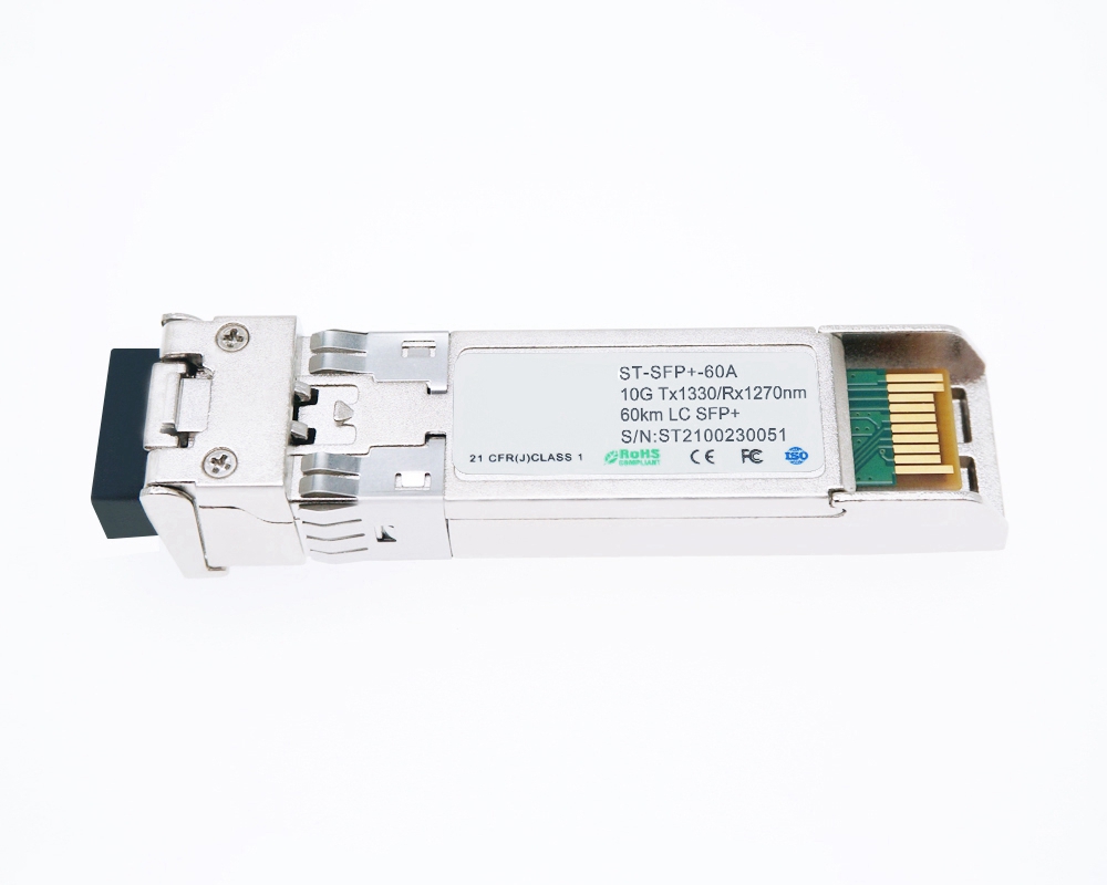
ST-XFP-60A |
1270nm DFB laser Transmitter and 1330nm Receiver, XFP 10Gbps, 60km, 0ºC ~ +70ºC |
|
ST-XFP-60B |
1330nm DFB laser Transmitter and 1270nm Receiver, XFP 10Gbps, 60km, 0ºC ~ +70ºC |