Products+
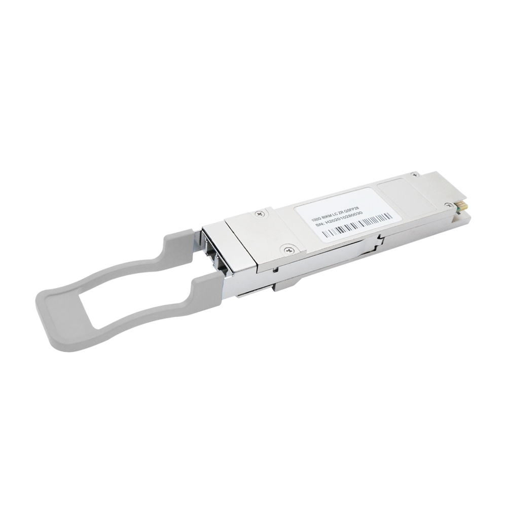
100Gb/s QSFP28 ZR4 Compatible Transceiver
100Gb/s QSFP28 ZR4 Transceiver, fully tested compatible for over 100 vendors.
Features
lCompliant with 100GBASE-ZR4
lSupport line rates from 103.125 Gb/s to 111.81 Gb/s OTU4
lLAN WDM EML laser and PIN receiver with SOA
lUp to 80km reach for G.652 SMF
lHot pluggable 38 pin electrical interface
lQSFP28 MSA compliant
lDuplex LC optical receptacle
lRoHS-10 compliant and lead-free
lSingle +3.3V power supply
lMaximum power consumption 6.5W
lCase operating temperature Commercial: 0 ~ +70℃ Extended-10 ~ +80℃
Industrial: -40 ~ +85℃
General Description
The transceiver is designed for 80km optical communication applications. This module contains 4-lane optical transmitter, 4-lane optical receiver and module management block including 2 wireserial inter- face. The optical signals are multiplexed to a single-mode fiber through an industry standard LC connector. A block diagram is shown in Figure 1
ModSeIL
The ModSelL is an input pin. When held low by the host, the module responds to 2-wire serial communication commands. The ModSelL allows the use of multiple modules on a single 2-wire interface bus. When the ModSelL is "High", the module shall not respond to or acknowledge any 2-wire interface communication from the host. ModSelL signal input node shall be biased to the "High" state in the module.
In order to avoid conflicts, the host system shall not attempt 2-wire interface communicationswithin the ModSelL de-assert time after any modules are deselected. Similarly, the host shall wait at least for the period of the ModSelL assert time before communicating with the newly selected module. The assertion and de-asserting periods of different modules may overlap as long as the above timing requirements are met.
Absolute Maximum Ratings
It has to be noted that the operation in excess of any individual absolute maximum ratings might cause permanent damage to this module.
|
Parameter |
Symbol |
Min |
Max |
Unit |
Notes |
|
Storage Temperature |
TS |
-40 |
85 |
oC |
|
|
Power Supply Voltage |
VCC |
-0.3 |
4.0 |
V |
|
|
Relative Humidity (non-condensation) |
RH |
15 |
85 |
% |
|
|
Damage Threshold |
THd |
6.5 |
|
dBm |
|
Recommended Operating Conditions
|
Parameter |
Symbol |
Min |
Typical |
Max |
Unit |
Notes |
|
Operating Case Temperature |
TOP |
0 |
|
70 |
oC |
commercial |
|
-10 |
|
80 |
extended |
|||
|
-40 |
|
85 |
Industrial |
|||
|
Power Supply Voltage |
VCC |
3.135 |
3.3 |
3.465 |
V |
|
|
Data Rate, each Lane |
|
|
25.78125 |
|
Gb/s |
|
|
Control Input Voltage High |
|
2 |
|
Vcc |
V |
|
|
Control Input Voltage Low |
|
0 |
|
0.8 |
V |
|
|
Link Distance (SMF) |
D |
|
|
80 |
km |
1 |
Notes:
- Depending on actual fiber loss/km (link distance specified is for fiber insertion loss of 0.35dB/km)
Electrical Characteristics
The following electrical characteristics are defined over the Recommended Operating Environment unless otherwise specified.
|
Common Mode conversion (SDC11, SCD11) |
|
|
|
-VSR Equation 13-20 |
|
|
|
Stressed Input Test |
TP1a |
See CEI-28G -VSR Section 13.3.11. 2.1 |
|
|
|
|
|
Receiver |
||||||
|
Differential Voltage, pk-pk |
TP4 |
|
|
900 |
mV |
|
|
Common Mode Voltage (Vcm) |
TP4 |
-350 |
|
2850 |
mV |
1 |
|
Common Mode Noise, RMS |
TP4 |
|
|
10 |
% |
At 1MHz |
|
Differential Return Loss (SDD22) |
TP4 |
|
|
See CEI-28G -VSR Equation 13-19 |
dB |
|
|
Common Mode to Differential conversion and Differential to Common Mode conversion (SDC22, SCD22) |
TP4 |
|
|
See CEI-28G -VSR Equation 13-21 |
dB |
|
|
Common Mode Return Loss (SCC22) |
TP4 |
|
|
-2 |
dB |
2 |
|
Transition Time, 20 to 80% |
TP4 |
9.5 |
|
|
ps |
|
|
Vertical Eye Closure (VEC) |
TP4 |
|
|
5.5 |
dB |
|
|
Eye Width at 10-15 probability (EW15) |
TP4 |
0.57 |
|
|
UI |
|
|
Eye Height at 10-15 probability (EH15) |
TP4 |
228 |
|
|
mV |
|
Notes:
- Vcm is generated by the host. Specification includes effects of ground offset
- From 250MHz to
Optical Characteristics
The following optical characteristics are defined over the Recommended Operating Environment unless otherwise specified.
|
Parameter |
Symbol |
Min. |
Typical |
Max |
Unit |
Notes |
|
Transmitter |
||||||
|
Lane wavelength(range) |
L0 |
1294.53 |
1295.56 |
1296.59 |
nm |
|
|
L1 |
1299.02 |
1300.05 |
1301.09 |
nm |
|
|
|
L2 |
1303.54 |
1304.58 |
1305.63 |
nm |
|
|
|
L3 |
1308.09 |
1309.14 |
1310.09 |
nm |
|
|
|
Signaling rate, each lane |
|
|
25.78125 |
|
GBd |
|
|
Side-mode suppression ratio |
SMSR |
30 |
|
|
|
|
|
Total launch power |
PT |
8.0 |
|
12.5 |
dBm |
|
|
Average launch power, each lane |
Pavg |
2.0 |
|
4.5 |
dBm |
1 |
|
OMA, each Lane |
POMA |
0.1 |
|
4.5 |
dBm |
2 |
|
Extinction Ratio |
ER |
6.0 |
|
|
dB |
|
|
Difference in Launch Power between any Two Lanes (OMA) |
Ptx,diff |
|
|
3.6 |
dB |
|
|
Transmitter and Dispersion Penalty, each lane |
TDP |
|
|
2.5 |
dB |
|
|
OMA minus TDP, each lane |
OMA-TD P |
-0.65 |
|
|
dBm |
|
|
Average launch power of OFF transmitter, each lane |
Poff |
|
|
-30 |
dBm |
|
|
Transmitter reflectance |
RT |
|
|
-12 |
dB |
|
|
RIN20OMA |
RIN |
|
|
-130 |
dB/Hz |
|
|
Optical Return Loss Tolerance |
TOL |
|
|
20 |
dB |
|
|
Transmitter eye mask {X1, X2,X3, Y1, Y2, Y3} |
|
{0.25, 0.4, 0.45, 0.25, 0.28, 0.4} |
|
|
||
|
Receiver |
||||||
|
Signaling rate, each lane |
|
|
25.78125 |
|
GBd |
|
|
Average Receive Power, each Lane |
|
-28 |
|
-3.5 |
dBm |
|
|
Receive Power (OMA), each Lane |
|
|
|
-3.5 |
dBm |
|
|
Receiver reflectance |
SEN1 |
|
|
-26 |
dBm |
for BER = 1x10-12 |
|
Receiver sensitivity Average, each lane |
SEN2 |
|
|
-28 |
dBm |
for BER = 5x10⁻⁵ |
|
Difference in Receive Power between any Two Lanes (Average and OMA) |
Ptx,diff |
|
|
3.6 |
dB |
|
|
LOS Assert |
LOSA |
-40 |
|
|
dBm |
|
|
LOS Deassert |
LOSD |
|
|
-29 |
dBm |
|
|
LOS Hysteresis |
LOSH |
0.5 |
|
|
dB |
|
|
Conditions of Stress Receiver Sensitivity Test (Note 4) |
||||||
|
Vertical Eye Closure Penalty, each Lane |
|
|
1.5 |
|
dB |
|
|
Stressed Eye J2 Jitter, each Lane |
|
|
0.3 |
|
UI |
|
|
Stressed Eye J9 Jitter, each Lane |
|
|
0.47 |
|
UI |
|
Notes:
- The minimum average launch power spec is based on ER not exceeding 9.5dB and transmitter OMA higher than1dBm.
- Even if the TDP < 0.75 dB, the OMA min must exceed the minimum value specified