Products+
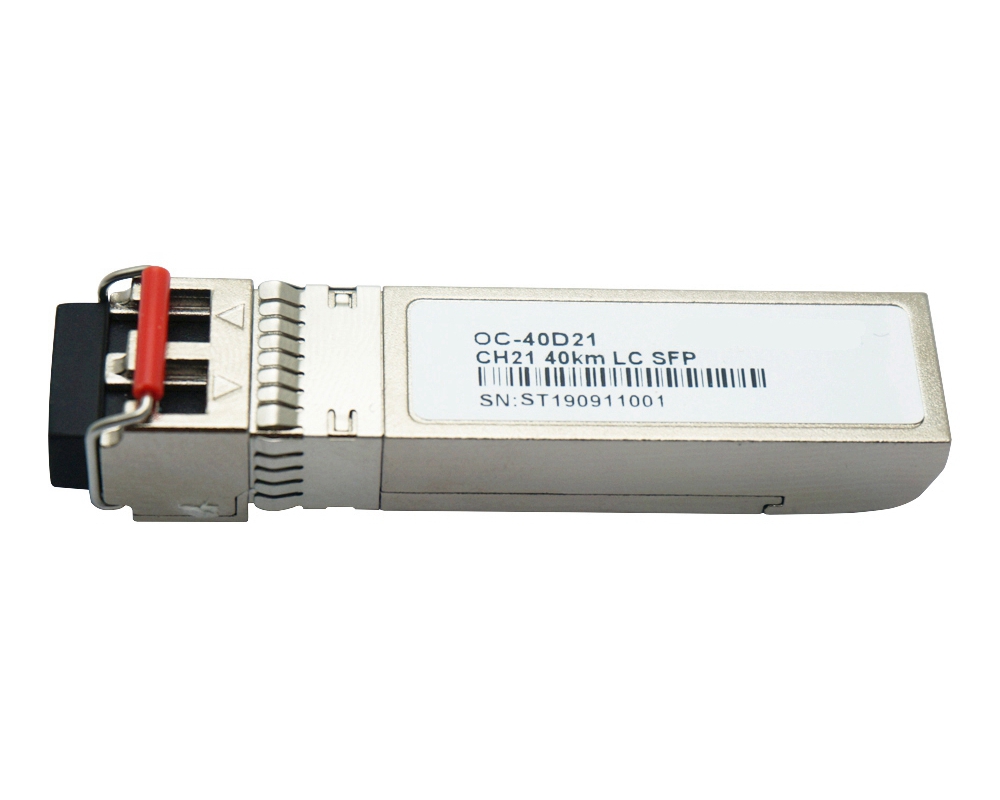
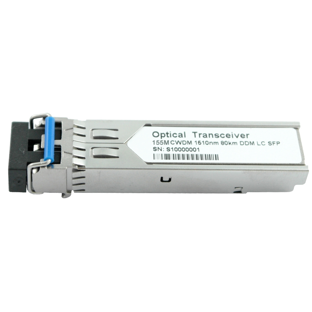
1.25G DWDM compatible SFP Optical Transceiver
1.25G DWDM SFP Optical Transceiver, 80- 120km reach,fully tested compatible for over 100 vendors.
Features
* Wavelength selectable to C-band and L-band ITU-T grid wavelengths
* Suitable for use in 100GHz channel spacing DWDM systems
* DWDM SFP MSA Compliant
* Up to 2. 667Gb/s data rate
* Cold Start up Wavelength Compliance
* Low Power Dissipation <1.3W Maximum
* 0ºC to 70ºC Operating Case Temperature
* Diagnostic Performance Monitoring of module temperature, supply
Voltages, laser bias current, transmit optical power, receive optical power,
Laser temperature and TEC current
* Extended link budget with APD receiver technology
* Long Reach 80km(1600 ps/nm), 120km(2400 ps/nm) Versions
* RoHS compliant and lead free
Applications
* SFP Transceivers for DWDM SONET/ SDH
* Ethernet IEEE 802.3ae
* Fiber Channel
Description
DWDM SFP Transceiver exhibits excellent wavelength stability, supporting operation at 100 GHz channel, cost effective module. It is designed for DWDM SONET/ SDH, Gigabit Ethernet and Fiber- Channel applications.
The transceiver consists of two sections: The transmitter section incorporates a colded DFB laser. And the receiver section consists of a APD photodiode integrated with a TIA. All modules satisfy class I laser safety requirements. DWDM SFP transceiver provides an enhanced monitoring interface, which allows real-time access to device operating parameters such as transceiver temperature, laser bias current, transmitted optical power, received optical power and transceiver supply voltage, laser temperature and TEC current.
Absolute Maximum Ratings
|
Parameter |
Symbol |
Min |
Max |
Unit |
|
Supply Voltage |
Vcc |
-0.3 |
4.0 |
V |
|
Storage Temperature |
Tst |
-40 |
85 |
ºC |
|
Data AC Voltage |
TX+-AC |
- |
2.4 |
Vpp |
|
Data DC Voltage |
TX+-DC |
-0.5 |
2.5 |
V |
|
Optical Input Received Power |
PIN |
- |
+5 |
dBm |
Operating Conditions
|
Parameter |
Symbol |
Min |
Typical |
Max |
Unit |
|
Supply Voltage |
Vcc |
3.13 |
3.3 |
3.47 |
V |
|
Operating Case temperature |
Tca |
-5 |
- |
70 |
ºC |
|
Total Current |
Icc |
- |
- |
380 |
mA |
|
Module Power Dissipation |
Pm |
- |
0.8 |
1.3 |
W |
Transmitter Specifications – Optical
|
Parameter |
Symbol |
Min |
Typical |
Max |
Unit |
|
Data Rate multi-rate |
Mra |
155 |
2488 |
2667 |
Mbps |
|
Center Wavelength (SOL)△ |
c |
c -25 |
c |
c +25 |
pm |
|
Center Wavelength (EOL)▲ |
c |
c -100 |
c |
c+100 |
pm |
|
Optical Transmit Power |
Po |
0 |
2 |
4 |
dBm |
|
Optical Transmit Power (disabled) |
PTX_DISABLE |
- |
- |
-40 |
dBm |
|
Extinction Ratio |
ER |
8.2 |
|
- |
dB |
|
Channel Spacing |
∆f |
- |
100 |
- |
GHz |
|
Jitter Generation |
TJP-P |
- |
- |
70 |
mUI |
|
Spectral Width (-20dB) |
Dl20 |
- |
0.1 |
0.3 |
nm |
|
Side Mode Suppression Ratio |
SMSR |
30 |
- |
- |
dB |
|
Eye Mask |
Compliant with Bell core GR-253-CORE & ITU G.957 for SONET/SDH and with IEEE 802.3ae for Ethernet and Fibre Channel |
||||
△Laser- Start of Life
▲Laser End of life
Transmitter Specifications – Electrical
|
Parameter |
Symbol |
Min |
Typical |
Max |
Unit |
|
Supply Voltage |
VccTX |
3.13 |
3.3 |
3.47 |
V |
|
PECL/CML Input |
VtxDIFF |
500 |
- |
1600 |
mV |
|
Input Rise/Fall |
TR / TF |
- |
- |
160 |
ps |
|
TX-Fault Fault |
Vf |
2 |
- |
Vcc |
V |
|
TX-Fault Normal |
Vn |
Vee |
- |
Vee+0.5 |
V |
|
TX_DISABLE (asserted) |
VDH |
2 |
- |
Vcc |
V |
|
TX_DISABLE (negated) |
VDL |
Vee |
- |
Vee+0.8 |
V |
APD Receiver Specifications – Optical
|
Parameter |
Symbol |
Min |
Typical |
Max |
Unit |
|
Receiver Sensitivity(oc48) |
Rsens-1 |
- |
-30 |
-28 |
dBm |
|
Receiver Sensitivity (OSNR = 20dB) |
Rsens-2 |
- |
- |
-24 |
dBm |
|
Maximum Input Power |
RX-overload |
- |
- |
-7 |
dBm |
|
Input Operating Wavelength |
λ |
1528 |
- |
1564 |
nm |
|
Reflectance |
Rrx |
- |
- |
-27 |
dB |
|
Loss of Signal Asserted |
|
-40 |
- |
- |
dBm |
|
LOS De-Asserted |
|
- |
- |
-28 |
dBm |
|
LOS Hysteresis |
|
0.5 |
- |
- |
dB |
APD Receiver Specifications – Electrical
|
Parameter |
Symbol |
Min |
Typical |
Max |
Unit |
|
Supply Voltage |
VccRX |
3.13 |
3.3 |
3.47 |
V |
|
Differential Output Swing |
Vout P-P |
370 |
- |
2000 |
mV |
|
Rise/Fall Time |
Tr / Tf |
- |
- |
175 |
ps |
|
Loss of Signal –Asserted |
VOH |
2 |
- |
Vcc |
V |
|
Loss of Signal –Negated |
VOL |
Vee |
- |
Vee+0.5 |
V |
Low Speed Electrical Signal Timings
|
Parameter |
Symbol |
Min |
Typical |
Max |
Unit |
|
TX Disable Negate Time |
t-on |
- |
- |
20 |
ms |
|
TX Disable Assert Time |
t-off |
- |
- |
20 |
ms |
|
Time to initialize, including reset of TX_FAULT |
t_init
|
- |
- |
300 |
ms |
|
Start-up Time |
t_startup |
- |
- |
90 |
s |
|
TX_FAULT/INT Assert Time |
t_fault |
- |
- |
50 |
ms |
|
TX_DISABLE to Reset |
t_reset |
10 |
- |
- |
ms |
|
LOS Assert Time |
t_los_on |
- |
- |
100 |
us |
|
LOS Negate Time |
t_los_off |
- |
- |
100 |
us |
|
Serial ID Clock Rate |
f_serial_clock |
- |
- |
100 |
kHz |
C-band λc Wavelength Guide
|
ITU Channel Product Code |
Frequency(THz) |
Wavelength |
ITU Channel Product Code |
Frequency(THz) |
Wavelength |
|
17 |
191.7 |
1563.86 |
40 |
194.0 |
1545.32 |
|
18 |
191.8 |
1563.05 |
41 |
194.1 |
1544.53 |
|
19 |
191.9 |
1562.23 |
42 |
194.2 |
1543.73 |
|
20 |
192.0 |
1561.42 |
43 |
194.3 |
1542.94 |
|
21 |
192.1 |
1560.61 |
44 |
194.4 |
1542.14 |
|
22 |
192.2 |
1559.79 |
45 |
194.5 |
1541.35 |
|
23 |
192.3 |
1558.98 |
46 |
194.6 |
1540.56 |
|
24 |
192.4 |
1558.17 |
47 |
194.7 |
1539.77 |
|
25 |
192.5 |
1557.36 |
48 |
194.8 |
1538.98 |
|
26 |
192.6 |
1556.55 |
49 |
194.9 |
1538.19 |
|
27 |
192.7 |
1555.75 |
50 |
195.0 |
1537.40 |
|
28 |
192.8 |
1554.94 |
51 |
195.1 |
1536.61 |
|
29 |
192.9 |
1554.13 |
52 |
195.2 |
1535.82 |
|
30 |
193.0 |
1553.33 |
53 |
195.3 |
1535.04 |
|
31 |
193.1 |
1552.52 |
54 |
195.4 |
1534.25 |
|
32 |
193.2 |
1551.72 |
55 |
195.5 |
1533.47 |
|
33 |
193.3 |
1550.92 |
56 |
195.6 |
1532.68 |
|
34 |
193.4 |
1550.12 |
57 |
195.7 |
1531.90 |
|
35 |
193.5 |
1549.32 |
58 |
195.8 |
1531.12 |
|
36 |
193.6 |
1548.51 |
59 |
195.9 |
1530.33 |
|
37 |
193.7 |
1547.72 |
60 |
196.0 |
1529.55 |
|
38 |
193.8 |
1546.92 |
61 |
196.1 |
1528.77 |
|
39 |
193.9 |
1546.12 |
|
|
|
L-band λc Wavelength Guide
|
ITU Channel Product Code |
Frequency(THz) |
Wavelength |
ITU Channel Product Code |
Frequency(THz) |
Wavelength |
|
62 |
186.2 |
1610.06 |
90 |
189.0 |
1586.20 |
|
63 |
186.3 |
1609.19 |
91 |
189.1 |
1585.36 |
|
64 |
186.4 |
1608.33 |
92 |
189.2 |
1584.53 |
|
65 |
186.5 |
1607.47 |
93 |
189.3 |
1583.69 |
|
66 |
186.6 |
1606.61 |
94 |
189.4 |
1582.85 |
|
67 |
186.7 |
1605.74 |
95 |
189.5 |
1582.02 |
|
68 |
186.8 |
1604.88 |
96 |
189.6 |
1581.18 |
|
69 |
186.9 |
1604.03 |
97 |
189.7 |
1580.35 |
|
70 |
187.0 |
1603.17 |
98 |
189.8 |
1579.52 |
|
71 |
187.1 |
1602.31 |
99 |
189.9 |
1578.69 |
|
72 |
187.2 |
1601.46 |
00 |
190.0 |
1577.86 |
|
73 |
187.3 |
1600.60 |
01 |
190.1 |
1577.03 |
|
74 |
187.3 |
1599.75 |
02 |
190.2 |
1576.20 |
|
75 |
187.5 |
1598.89 |
03 |
190.3 |
1575.37 |
|
76 |
187.6 |
1598.04 |
04 |
190.4 |
1574.54 |
|
77 |
187.7 |
1597.19 |
05 |
190.5 |
1573.71 |
|
78 |
187.8 |
1596.34 |
06 |
190.6 |
1572.89 |
|
79 |
187.9 |
1595.49 |
07 |
190.7 |
1572.06 |
|
80 |
188.0 |
1594.64 |
08 |
190.8 |
1571.24 |
|
81 |
188.1 |
1593.79 |
09 |
190.9 |
1570.42 |
|
82 |
188.2 |
1592.95 |
10 |
191.0 |
1569.59 |
|
83 |
188.3 |
1592.10 |
11 |
191.1 |
1568.77 |
|
84 |
188.4 |
1591.26 |
12 |
192.2 |
1567.95 |
|
85 |
188.5 |
1590.41 |
13 |
192.3 |
1567.13 |
|
86 |
188.6 |
1589.57 |
14 |
191.4 |
1566.31 |
|
87 |
188.7 |
1588.73 |
15 |
191.5 |
1565.50 |
|
88 |
188.8 |
1587.88 |
16 |
191.6 |
1564.68 |
|
89 |
188.9 |
1587.04 |
|
|
|
Table 1: EEPROM Serial ID Memory Contents (A0h):
|
Data Address |
Field Size (Bytes) |
Value |
Name of Field |
Description and Contents |
|
Base ID Fields |
||||
|
0 |
1 |
0Bh |
Identifier |
Type of Serial transceiver |
|
1 |
1 |
24h |
Ext. Identifier |
Extended identifier of type serial transceiver |
|
2 |
1 |
07h |
Connector |
Code of optical connector type |
|
3-10 |
8 |
00h,0Ch,44h,00h, 80h,10h,01h,00h |
Transceiver |
Code for electronic compatibility or optical compatibility |
|
11 |
1 |
03h |
Encoding |
Code for serial encoding algorithm |
|
12 |
1 |
19h |
BR,Nominal |
Nominal baud rate, unit of 100Mbps |
|
13-14 |
2 |
78h(120km) |
Length (9µm) – km |
Link length supported for 9/125µm fiber, units in km |
|
15 |
1 |
46h |
Max Temp |
Maximum operating case temperature in °C |
|
16 |
1 |
FBh |
Min Temp |
Minimum operating case temperature in °C |
|
17 |
1 |
5Fh |
Max Supply Current |
Maximum supply current in units of 4mA |
|
18 |
1 |
00h |
Reserved |
- |
|
19 |
1 |
41h |
Channel spacing and number |
Channel spacing compatibility and number and tuning of ITU channels supported |
|
20-35 |
16 |
Module dependent |
Vendor Name |
SFP vendor name: “BTON” |
|
36 |
1 |
02h |
Reserved |
Optional DWDM features |
|
37-39 |
3 |
- |
Vendor OUI |
SFP transceiver vendor IEEE company ID |
|
40-55 |
16 |
DWDM-XX-XX-XX |
Vendor PN |
Part number provided by SFP transceiver vendor (ASCII) |
|
56-59 |
4 |
Module dependent |
Vendor rev |
Revision level for part number provided by vendor (ASCII) |
|
60-61 |
2 |
Module dependent |
wavelength |
Laser wavelength (in nm) |
|
62 |
1 |
Module dependent |
wavelength |
Laser wavelength (fractional part in units of 10pm) |
|
63 |
1 |
Module dependent |
CC_BASE |
Check sum of bytes 0 - 62 |
|
Extended ID Fields |
||||
|
64-65 |
2 |
1Ah |
Option |
Indicates which optical SFP signals are implemented |
|
66 |
1 |
00h |
BR, max |
Upper bit rate margin, units of % |
|
67 |
1 |
00h |
BR, min |
Lower bit rate margin, units of % |
|
68-83 |
16 |
Module dependent |
Vendor SN |
Serial number (ASCII) |
|
84-91 |
8 |
Module dependent |
Date code |
Year(2 bytes), Month(2 bytes), Day (2 bytes) |
|
92 |
1 |
68h |
Diagnostic type |
Indicates the type of diagnostics implemented in Monitoring Type the transceiver |
|
93 |
1 |
F0h |
Enhanced option |
Indicates which optional enhanced features Options are implemented |
|
94 |
1 |
01h |
SFF-8472 |
“01” Diagnostics(SFF-8472 Rev 9.3) |
|
95 |
1 |
Module dependent |
CC_EX |
Check sum of bytes 64 - 94 |
|
Vendor Specific ID fields |
||||
|
96-127 |
32 |
- |
Vendor Specific |
Vendor Specific EEPROM (Vendor specific data; Specific read only) |
|
128-255 |
128 |
- |
Reserved |
Reserved for future use |
Table 2: Serial ID Memory Contents: (A2H)
|
Address |
# Bytes |
Name |
Description |
|
00-55 |
56 |
Alarm and Warning Levels |
Temp/ Vcc/ Bias Current /TX Power/ RX Power/ LD Temp/ TEC Current, High/Low Alarm and Warning Levels |
|
56-94 |
39 |
|
Not used in DWDM devices. All Bytes Set to 0. |
|
95 |
1 |
Checksum |
Low order 8 bits of the sum of bytes 0-94 |
|
96-109 |
8 |
A/D Values |
A/D binary values of the following enhanced diagnostics(Real-time): module temperature, supply voltage, laser bias current, transmit optical power, receive optical power, laser temperature and TEC current. These values are Internally calibrated absolute measurements. All diagnostic parameters implemented in these address locations have a corresponding high and low, alarm and warning thresholds assigned in address locations 00-55. |
|
110 |
1 |
Soft Control Signals |
Soft control signals monitored over the 2-wire access port. can updated real-time status of the following control signals: TX_FAULT, TX_DISABLE, Rate Select, and LOS. |
|
111 |
1 |
Reserved |
Reserved |
|
112-117 |
5 |
Alarm/Warning Flags |
Optional Alarm and Warning Flag and Mask Bits Corresponding to levels detailed in addresses 00-39 above. |
|
118-119 |
2 |
Warning Mask |
Masking bits corresponding to Warning bits of bytes 116 and 117 respectively |
|
120-126 |
8 |
Vendor Specific |
Vendor specific data |
|
127 |
1 |
Table Select |
The byte value defines the Table location for subsequent reads and writes to bytes locations 128-255 |
|
128-247 |
120 |
User EEPROM |
User writable EEPROM |
|
248-255 |
8 |
Vendor Specific |
Vendor specific control functions |
Table 3: Digital Diagnostic Monitoring A/D Accuracy
|
Parameter |
Range |
Accuracy |
Unit |
|
Temperature |
-40~100 |
± 3 |
℃ |
|
Voltage |
0~Vcc |
0.1 |
V |
|
Bias Current |
0~120 |
5 |
mA |
|
TX Power |
0~5 |
± 2 |
dBm |
|
RX Power |
-32~-8 |
± 2 |
dBm |
|
TEC Current |
-1200~1200 |
± 65 |
mA |
|
LD Temperature |
20~70 |
± 0.25 |
℃ |
Pin Definitions
|
Pin Number |
Name |
Function |
Ref. |
|
1 |
VEET |
Transmitter Ground |
|
|
2 |
TX_FAULT/INT |
Transmitter Fault |
1 |
|
3 |
TX_DISABLE |
Transmitter Disable |
2 |
|
4 |
MOD-DEF(2) |
Module Definition 2 |
3 |
|
5 |
MOD-DEF(1) |
Module Definition 1 |
3 |
|
6 |
MOD-DEF(0) |
Module Definition 0 |
3 |
|
7 |
Tone in |
Rate Select -Not Implemented |
|
|
8 |
LOS |
Loss of Signal |
4 |
|
9 |
VEER |
Receiver Ground |
|
|
10 |
VEER |
Receiver Ground |
|
|
11 |
VEER |
Receiver Ground |
|
|
12 |
RD- |
Inverted Received |
|
|
13 |
RD+ |
Received Data |
|
|
14 |
VEER |
Receiver Ground |
|
|
15 |
VCCR |
Receiver Power |
|
|
16 |
VCCT |
Transmitter Power |
|
|
17 |
VEET |
Transmitter Ground |
|
|
18 |
TD+ |
Transmit Data |
|
|
19 |
TD- |
Inverted Transmit |
|
|
20 |
VEET |
Transmitter Ground |
|
Notes:
- TX Fault is an open collector/drain output, which should be pulled up with a 4.7K – 10K. resistor on the host board. Pull up voltage between 2.0V and VccT, R+0.3V. When high, output indicates a laser fault of some kind. Low indicates normal operation. In the low state, the output will be pulled to < 0.8V.
- TX disable is an input that is used to shut down the transmitter optical output. It is pulled up within the module with a 4.7 – 10 K. resistor.
- These are the module definition pins. They should be pulled up with a 4.7K – 10K. resistor on the host board. The pull-up voltage shall be VccT or VccR (see Section IV for further details).
- LOS (Loss of Signal) is an open collector/drain output, which should be pulled up with a 4.7K – 10K. resistor. Pull up voltage between 2.0V and VccT, R+0.3V. When high, this output indicates the received optical power is below the worst-case receiver sensitivity (as defined by the standard in use). Low indicates normal operation. In the low state, the output will be pulled to < 0.8V.